一般请人做网站和app多少钱国内新闻最新消息10条
🎈 概述
当我们想提供可靠的 API 接口,对参数的校验,以保证最终数据入库的正确性,是 必不可少 的活。比如下图就是 我们一个项目里 新增一个菜单校验 参数的函数,写了一大堆的 if else 进行校验,或者基础校验,如非空校验、长度校验、大小校验、格式校验;也有一些校验是业务校验,如学号不能重重复、手机号不能重复注册等,非常的不优雅,比起枯燥的CRUD来说,参数校验更是枯燥。例:
/** * 参数校验* @param user* @return void * @author PuWenshuo* @date 2023/4/26 11:08*/ private void verifyForm(SysUser user){if(StringUtils.isBlank(user.getUserName())){throw new RuntimeException("用户名称不能为空");}if(user.getDeptId() == null){throw new RuntimeException("用户部门ID不能为空");}if(StringUtils.isBlank(user.getAvatar())){throw new RuntimeException("用户头像不能为空");}if(StringUtils.isBlank(user.getEmail())){throw new RuntimeException("用户邮箱不能为空");}if(StringUtils.isBlank(user.getPhonenumber())){throw new RuntimeException("用户手机号不能为空");}if(StringUtils.isBlank(user.getPassword())){throw new RuntimeException("用户密码不能为空");}}
🎈 引入依赖
在 Spring Boot 体系中,也提供了 spring-boot-starter-validation 依赖。在这里,我们并没有引入。为什么呢?因为 spring-boot-starter-web 已经引入了 spring-boot-starter-validation ,而 spring-boot-starter-validation 中也引入了 hibernate-validator 依赖,所以无需重复引入。
<dependency><groupId>org.springframework.boot</groupId><artifactId>spring-boot-starter</artifactId>
</dependency>
<dependency><groupId>org.springframework.boot</groupId><artifactId>spring-boot-starter-web</artifactId>
</dependency>
<dependency><groupId>org.springframework.boot</groupId><artifactId>spring-boot-starter-validation</artifactId><version>2.3.9.RELEASE</version>
</dependency>
🎈 注解
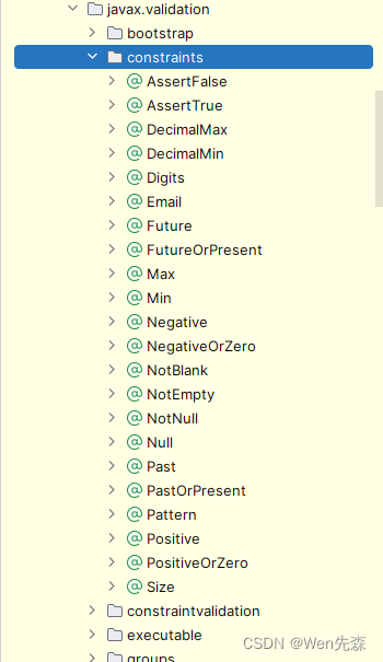
引入依赖后,可以看到在javax.validation.constraints 包下,定义了一系列的约束( constraint )注解。共 22个,如下:
💧 空和非空检查
@Null:被注释的元素必须为 null。@NotNull:被注释的元素必须不为 null。@NotEmpty:被注释的字符串的必须非空,集合对象的元素不为 0 ,即集合不为空。@NotBlank:只能用于字符串不为 null ,并且字符串trim()以后 length 要大于 0 。
💧 数值检查
@DecimalMax(value):被注释的元素必须是一个数字,其值必须小于等于指定的最大值。@DecimalMin(value):被注释的元素必须是一个数字,其值必须大于等于指定的最小值。@Digits(integer, fraction):被注释的元素必须是一个数字,其值必须在可接受的范围内。@Positive:判断正数。@PositiveOrZero:判断正数或 0 。@Max(value):该字段的值只能小于或等于该值。@Min(value):该字段的值只能大于或等于该值。@Negative:判断负数。@NegativeOrZero:判断负数或 0 。
💧 Boolean 值检查
@AssertFalse:被注释的元素必须为 true 。@AssertTrue:被注释的元素必须为 false 。
💧 长度检查
@Size(max, min):检查该字段的 size 是否在 min 和 max 之间,可以是字符串、数组、集合、Map 等。
💧 日期检查
@Future:被注释的元素必须是一个将来的日期。@FutureOrPresent:判断日期是否是将来或现在日期。@Past:检查该字段的日期是在过去。@PastOrPresent:判断日期是否是过去或现在日期。
💧 其它检查
@Email:被注释的元素必须是电子邮箱地址。@Pattern(value):被注释的元素必须符合指定的正则表达式。
💧 @Valid 和 @Validated
@Valid 注解,是 Bean Validation 所定义,可以添加在普通方法、构造方法、方法参数、方法返回、成员变量上,表示它们需要进行约束校验。
@Validated 注解,是 Spring Validation 锁定义,可以添加在类、方法参数、普通方法上,表示它们需要进行约束校验。同时,@Validated 有 value 属性,支持分组校验。属性如下:

@Valid(javax.validation包下) 和 @Validated(org.springframework.validation.annotation包下)注解。两者大致有以下的区别:
| 名称 | 是否实现声明式校验 | 是否支持嵌套校验 | 是否支持分组校验 |
|---|---|---|---|
@Valid | false | true | false |
@Validated | true | false | true |
绝大多数场景下,我们使用 @Validated 注解即可。而在有嵌套校验的场景,我们使用 @Valid 注解添加到成员属性上。
🎈 基本使用
参数校验分为简单校验、嵌套校验、分组校验。
💧 简单校验
简单校验直接在需要的实体类元素中标注约束注解即可。例如:
// 在实体类中添加各种不同的校验注解
@Data
public class UserRegisterDTO {@NotBlank(message = "用户名不能为空")private String username;@NotBlank(message = "密码不能为空")@Pattern(regexp = "^[0-9a-zA-Z]{6,16}$", message = "密码必须为 6-16 位的数字字母组合")private String password;@Email(message = "邮箱格式不正确")private String email;
}
注:同一个属性可以指定多个约束,比如@NotBlank和@Pattern,其中的message属性指定了约束条件不满足时的提示信息。
以上约束标记完成之后,要想完成校验,需要在controller层的接口标注@Valid注解即可。如下所示:
@RestController
@RequestMapping("/user")
public class UserController {@PostMapping("/register")public Result register(@RequestBody @Valid  UserRegisterDTO userRegisterDTO) {// 参数校验通过后的逻辑处理}}
💧 嵌套校验
在 Spring Boot 中,我们可以使用注解实现嵌套校验。嵌套校验主要是针对复杂的业务场景,例如一个对象中包含了另一个对象,或者一个集合中包含了多个元素等情况。
嵌套校验很简单,只需要在嵌套的实体属性标注@Valid注解,则其中的属性也将会得到校验,否则不会校验。
例如下面的实体类校验:
// 用户实体类
@Data
public class User {@NotNull(message = "用户名不能为空")private String username;@Size(min = 6, max = 20, message = "密码长度应在 6 到 20 之间")private String password;
}// 商品实体类
@Data
public class Product {@NotNull(message = "商品编号不能为空")private String productId;@NotEmpty(message = "商品名称不能为空")private String productName;@Positive(message = "商品价格必须为正数")private BigDecimal price;
}// 订单实体类  ,需要使用@Valid标注才能嵌套校验用户类和商品类
@Data
public class Order {@NotNull(message = "订单号不能为空")private String orderId;@Valid@NotNull(message = "订单用户信息不能为空")private User user;/*** @Valid这个注解标注在集合上,将会针对集合中每个元素进行校验*/@Valid@Size(min = 1,message = "至少一个商品")@NotEmpty(message = "订单商品列表不能为空")private List<Product> productList;
}则在Controller层的接口,需要使用@Valid或者@Validated标注入参,嵌套校验中仍可以使用分组校验。
@RestController
@RequestMapping("/order")
public class OrderController {@PostMapping("/add")public void addOrder(@RequestBody @Valid  Order order) {// 业务处理}}
总结:嵌套校验只需要在需要校验的元素(单个或者集合)上添加@Valid注解,接口层需要使用@Valid或者@Validated注解标注入参。
💧 分组校验
有的时候,开发者在某一个实体类中定义了很多校验规则,但是在某一次业务处理中,并不需要这么多校验规则,此时就可以使用分组校验:
首先创建两个分组接口:
public interface AddGroup {}public interface UpdateGroup {}
在实体类中添加分组信息:
@Data
public class User {/*** groups属性,表示该校验属性规则所属的分组*/@NotNull(message = "用户名不能为空", groups = {UpdateGroup.class})private String id;@NotNull(message = "用户名不能为空", groups = {AddGroup.class, UpdateGroup.class})private String username;@Size(min = 6, max = 20, message = "密码长度应在 6 到 20 之间", groups = {AddGroup.class})private String password;@Email(message = "邮箱格式不正确")private String email;
}
在在Controller层的接口使用@Validated注解中指定校验分组:
@RestController
@RequestMapping("/user")
public class UserController {@PostMapping("/add")public void addUser(@RequestBody @Validated(AddGroup.class) User user) {// 业务处理}/*** @Validated({UpdateGroup.class, Default.class})表示UpdateGroup和默认分组都参与校验*/@PostMapping("/update")public void updateUser(@RequestBody @Validated({UpdateGroup.class, Default.class}) User user) {// 业务处理}}
💧 @RequestBody注解参数
在 Spring Boot 中,我们可以使用 @RequestBody 注解来接收请求体中的参数,并对其进行校验。通常情况下,我们会使用 javax.validation.constraints 包提供的注解来对请求参数进行校验。
下面是一个示例,展示如何使用 @RequestBody 注解和校验注解来对请求参数进行校验:
@RestController
public class UserController {@PostMapping("/user")public User addUser(@Validated @RequestBody User user) {return user;}}
在上面的例子中,我们定义了一个 addUser() 方法,并使用 @RequestBody 注解来接收请求体中的参数,这里的参数类型是 User 类型。然后,我们使用 @Validated 注解来告诉 Spring Boot 对请求参数进行校验,同时,在 User 类中使用校验注解进行参数校验,例如 @NotBlank、@NotNull、@Min、@Max 等等。
举个例子,假设我们的 User 类如下所示:
@Data
public class User {@NotBlank(message = "用户名不能为空")private String username;@NotBlank(message = "密码不能为空")private String password;@Email(message = "邮箱格式不正确")private String email;
}
在上面的例子中,我们在 User 类中添加了几个校验注解来校验请求参数的合法性,例如 @NotBlank 来判断参数是否为空或空格,@Email 来判断邮箱格式是否正确等等。
当客户端发起 POST 请求时,请求体中包含一个合法的 User 对象,Spring Boot 会自动对其进行校验。如果请求参数不符合规范,则会抛出相应的异常(例如 MethodArgumentNotValidException),并返回给客户端相应的错误信息。
总结:
- 在controller层的方法的形参数前面加一个@Valid或@Validated的注解;
- 在用@RequestBody修饰的类的属性上加上约束注解,如@NotNull、@Length、@NotBlank;
- @RequestBody参数在触发校验规则时,会抛出MethodArgumentNotValidException,这里使用统一的异常处理机制来处理异常;
💧 @RequestParam注解/@PathVariable注解参数
在 Spring Boot 中,如果需要对 @RequestParam 参数和 @PathVariable 参数进行校验,我们通常会使用 javax.validation.constraints 提供的注解来实现。如果我们在控制类中使用注解进行参数校验,那么我们需要在该类上添加 @Validated 注解来开启校验功能。
例如:
@RestController
@Validated
public class UserController {@GetMapping("/user/{id}")public User getUser(@PathVariable("id") @Min(1) Long id) {// 业务逻辑}@PostMapping("/user")public void addUser(@RequestParam("username") @NotBlank String username, @RequestParam("password") @Size(min = 6, max = 20) String password) {// 业务逻辑}}
在上面的例子中,我们在 @PathVariable 和 @RequestParam 参数上分别添加了校验注解,例如 @Min、@NotBlank、@Size 等等。同时,我们在控制类上添加了 @Validated 注解来开启校验功能。
需要注意的是,在使用 @Validated 注解时,我们应该将其添加在控制类的上方,而不是方法上方。这是因为,当我们在方法上方添加 @Validated 注解时,将只会对该方法的参数进行校验,而不会校验控制类中其他方法的参数。
总之,如果需要对 @RequestParam 参数和 @PathVariable 参数进行校验,我们可以在控制类中使用校验注解来实现,并在控制类上添加 @Validated 注解开启校验功能。如果校验失败,则 Spring 会抛出 MethodArgumentNotValidException 异常,并将错误信息封装成 BindingResult 对象返回给控制层。
🎈 异常处理
既然是校验参数,有校验通过自然也就有不通过,如果参数校验失败,框架会自动抛出异常。对于异常可以通过两种方式处理:BindingResult 接收和全局捕获异常
💧 BindingResult 接收
在 Spring Boot 中,校验注解对请求参数进行校验时,当校验失败时,框架会将错误信息绑定到 BindingResult对象中,并将该对象作为方法参数传递给控制器方法。我们可以通过BindingResult对象获取到校验结果和错误信息,并进行相应的处理。
下面是一个示例,展示如何使用 BindingResult 对象接收参数校验异常:
@RestController
public class UserController {@PostMapping("/user")public void addUser(@Validated @RequestBody User user, BindingResult result) {if (result.hasErrors()) {List<String> errorMessages = new ArrayList<>();for (FieldError fieldError : result.getFieldErrors()) {String errorMessage = String.format("%s:%s", fieldError.getField(), fieldError.getDefaultMessage());errorMessages.add(errorMessage);}throw new RuntimeException(StringUtils.join(errorMessages, ";"));}// 接口正常的业务逻辑}}
在上面的例子中,我们定义了一个控制器方法 addUser,用来添加用户信息。我们在方法参数前添加了 @Validated 注解,表示需要对该参数进行校验。同时,我们还在方法的参数列表中添加了 BindingResult 参数,用来接收校验结果和错误信息。
在方法体内,我们首先使用 result.hasErrors() 判断是否存在校验错误。如果存在校验错误,我们遍历 FieldError 集合获取每个参数的校验错误信息,并将其封装到一个字符串列表 errorMessages 中。最后,我们将所有错误信息使用分号 ; 连接起来,并通过抛出运行时异常的方式将错误信息抛出。
需要注意的是,当我们使用 BindingResult 接收校验结果时,我们应该提供明确的错误提示信息,并避免返回给客户端过于详细的错误信息,以保障代码的安全性。
优点:使用 BindingResult 对象接收参数校验异常是一种比较简单和直接的方式,可以有效地处理参数校验异常,提高代码的健壮性和可靠性。
缺点:
- 当控制器方法参数列表中添加了 BindingResult 参数时,如果校验出错,框架不会抛出异常,而是将错误信息保存在 BindingResult 对象中返回到控制器方法中。因此,在处理校验结果时,我们需要手动判断是否存在校验错误,并获取校验错误信息。这会增加代码的复杂程度和维护成本。
- 使用 BindingResult 对象进行参数校验时,错误信息可能不够明确或不够详细,导致用户难以理解校验错误原因,从而无法快速定位问题所在。特别是当参数校验规则变得复杂时,错误信息可能不够准确或直观,使得调试和排查问题变得更加困难。
- 在使用 BindingResult 对象进行参数校验时,需要手动编写错误处理逻辑,并对校验结果进行详细的记录和分析,这会增加开发者的负担和工作量。
综上所述,虽然使用 BindingResult 对象进行参数校验可以有效地处理参数校验异常,但是它也存在一些缺点,例如代码复杂度高、错误信息不够明确等等。因此,在实际应用中,我们可以根据具体情况选择不同的方式来处理参数校验异常。如果需要更精准和明确的错误信息,可以使用 Spring Boot 中的全局异常处理器来处理参数校验结果。
💧 全局捕获异常处理
参数在校验失败的时候会抛出的MethodArgumentNotValidException或者BindException两种异常,可以在全局的异常处理器中捕捉到这两种异常,将提示信息或者自定义信息返回给客户端。
下面是一个示例,展示如何在 Spring Boot 中处理参数校验结果:
/*** 全局异常处理器* * @author Wen先森*/
@RestControllerAdvice
public class GlobalExceptionHandler
{private static final Logger log = LoggerFactory.getLogger(GlobalExceptionHandler.class);/*** 自定义验证异常*/@ExceptionHandler(BindException.class)public AjaxResult validatedBindException(BindException e){log.error(e.getMessage(), e);// 这里我只取了第一个错误信息。String message = e.getAllErrors().get(0).getDefaultMessage();// 同意返回前端错误信息处理return AjaxResult.error(message);}/*** 自定义验证异常*/@ExceptionHandler(MethodArgumentNotValidException.class)public Object validExceptionHandler(MethodArgumentNotValidException e){log.error(e.getMessage(), e);// getFieldError()不指定参数,会默认取第一个错误信息。String message = e.getBindingResult().getFieldError().getDefaultMessage();return AjaxResult.error(message);}
}
Spring Boot 提供了全局异常处理机制,可以通过 @ControllerAdvice 和 @ExceptionHandler 注解来处理控制器或服务中发生的异常。在上面的例子中,我们定义了一个全局异常处理器 GlobalExceptionHandler,用来捕获 MethodArgumentNotValidException 异常和BindException异常。e.getBindingResult()是获取到校验结果和错误信息即BindingResult 。
getFieldErrors() 和 getFieldError() 都是 Spring Boot 中用于获取校验错误信息的方法,但是它们的返回值和使用场景略有不同。
getFieldErrors() 方法可以获取到所有校验失败的错误信息,返回的是一个 List 集合,其中每个元素表示一个参数的校验错误信息。例如,我们可以使用以下代码获取到所有校验失败的参数信息:
BindingResult result = ... // 获取到绑定结果对象
List<FieldError> fieldErrors = result.getFieldErrors();
for (FieldError fieldError : fieldErrors) {String fieldName = fieldError.getField(); // 获取参数名String errorMsg = fieldError.getDefaultMessage(); // 获取错误信息// ...
}
getFieldErrors() 方法通常用来获取到所有校验失败的信息,并在控制器或服务中做进一步处理。例如,我们可以将所有的错误信息封装成一个响应对象并返回给客户端。
而 getFieldError() 方法则只能获取到某个具体参数的校验错误信息,返回的是一个 FieldError 对象,该对象包含了参数名、错误信息等详细信息。例如,我们可以使用以下代码获取到某个具体参数的校验错误信息:
BindingResult result = ... // 获取到绑定结果对象
FieldError fieldError = result.getFieldError("age"); // 获取 "age" 参数的错误信息
// 如果不指定参数,会默认获取第一个
// FieldError fieldError = result.getFieldError();
if (fieldError != null) {String fieldName = fieldError.getField(); // 获取参数名String errorMsg = fieldError.getDefaultMessage(); // 获取错误信息// ...
}
🎈 自定义校验
在Spring Boot中,可以通过自定义注解,并结合@Valid和@Validated注解来实现自定义校验。
💧 自定义校验注解
下面是一个简单的示例,展示如何自定义一个校验注解:
@Target({ METHOD, FIELD, ANNOTATION_TYPE, CONSTRUCTOR, PARAMETER, TYPE_USE })
@Retention(RUNTIME)
@Repeatable(List.class)
@Documented
@Constraint(validatedBy = MyValidator.class)// 指定校验器
public @interface MyConstraint {String message() default "自定义校验错误信息";Class<?>[] groups() default { };Class<? extends Payload>[] payload() default { };@Target({ METHOD, FIELD, ANNOTATION_TYPE, CONSTRUCTOR, PARAMETER, TYPE_USE })@Retention(RUNTIME)@Documented@interface List {MyConstraint [] value();}
}
这段代码定义了一个 MyConstraint(自定义注解)注解,它表示被注解的元素的值要小于等于指定的值。
注解应用于的元素类型包括:方法、字段、注解类型、构造函数、参数、类型使用。
@Retention(RUNTIME) 表示该注解在运行时可见,这样就可以使用反射机制来读取注解信息。
@Repeatable(List.class) 表示此注解可以重复标注在同一元素上,而多次使用该注解时,需要使用外部注解 List 来包装并保存多个 Max 注解的数组(具体实现请参考上面的问题解答)。
@Documented 表示该注解会包含在JavaDoc中。
注解中的属性包括:
- String message(),用于定义校验失败时的提示信息,默认为 “自定义校验错误信息”
- Class<?>[] groups(),用于将校验信息分组,方便给不同的校验规则分配到不同的分组中;
- Class<? extends Payload>[] payload(),用于在校验失败时传递的一些附加信息;
最后,该注解还内部定义了一个嵌套注解 List,用于表示被注解元素可以有多个MyConstraint(自定义注解)注解,通过 List 来包装这些注解,以此实现重复注解的功能。
我们还在 @MyConstraint 注解上加了 @Constraint(validatedBy = MyValidator.class) 注解,其中,validatedBy 属性指定了一个校验器类,该类需要实现 javax.validation.ConstraintValidator 接口,用于对注解进行具体的校验逻辑。
💧 自定义校验器
自定义校验注解的目的是为了自定义校验规则,而自定义校验器则是实现这种自定义校验规则的具体方式,在自定义注解中指定自定义校验器可以使得该注解在被使用时自动调用相应的校验器进行参数校验。
上面自定义检验注解时指定了校验器为MyValidator,自定义校验器需要实现ConstraintValidator<A extends Annotation, T>这个接口,第一个泛型是校验注解,第二个是参数类型。
接下来我们实现自定义检验器:
public class MyValidator implements ConstraintValidator<MyConstraint, Object> {@Overridepublic void initialize(MyConstraint constraintAnnotation) {// 可以在这里初始化校验器}@Overridepublic boolean isValid(Object value, ConstraintValidatorContext context) {// 在这里编写具体的校验逻辑if (value == null) {return true; // 如果校验的值为null,就不进行校验,交给@NotNull等其他校验注解处理}// 假设我们要校验字符串长度是否超过10个字符String str = (String) value;return str.length() <= 10;}
}
该自定义校验器实现了 ConstraintValidator 接口,并通过泛型 ConstraintValidator<MyConstraint, Object> 指定了被校验值的类型和自定义注解类型。在实现该接口的方法中,initialize方法可以用于从自定义注解中获取注解属性,而 isValid 方法则是实际进行校验的方法,其中第一个参数是被校验的值,第二个参数是校验上下文,可以用来设置校验失败时的错误信息。